Analog Devices: Regulation Loop Without a Resistive Divider
Written by Frederik Dostal, Power Management Expert
Abstract
A new control loop architecture is designed to generate very low noise voltages. This can be utilized by both linear and switching regulators. In addition to the low noise achieved, the level of noise becomes independent of the set output voltage. This also makes it possible to generate very low output voltages down to 0 V.
Power converters typically incorporate a control loop to maintain a set output voltage, irrespective of variations in input voltage or load current.
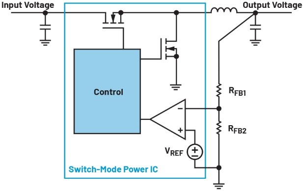
A resistor divider is often used to sense output voltage. One is depicted in Figure 1, which illustrates a step-down converting buck regulator circuit. In this control loop, a resistor divider (RFB1 and RFB2) adjusts the generated output voltage to a level specified by the internal reference voltage (VREF). This reference voltage is commonly set at 1.2 V, 0.8 V, or 0.6 V. The error amplifier’s output (operational amplifier in Figure 1) is then fed into a control block that manages the switching times of the power switches (MOSFETs).
Figure 1. The control loop of a power converter with a resistor divider.
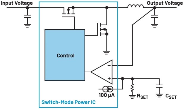
For a long time, this type of traditional regulation method was standard. However, a superior alternative now exists that offers many advantages for power conversion, including switching regulators and low dropout (LDO) regulators. Figure 2 shows the new concept, which employs a unity-gain architecture where the output voltage is fed directly to the error amplifier. The output voltage is adjusted with a resistor (RSET) connected to an internal power source. This configuration allows the output voltage to be adjusted down to 0 V, unlike the previous method using a resistor divider shown in Figure 1, where the minimum adjustable output voltage is equal to the potential of the internally installed reference voltage.
Another advantage is the ability to produce less noise at low frequencies below 100 kHz. By incorporating a CSET capacitance, it averages the low frequency disturbances from the internal current source, substantially reducing these interferences.
In this new architecture, the resistors of the resistor divider do not introduce additional noise, making the noise behavior largely independent of the output voltage. Consequently, the low frequency noise does not increase with higher output voltages.
Many of Analog Devices’ ultralow noise linear regulators, such as the LT3045 20 V, 500 mA ultralow noise LDO regulator, use this loop regulation technology. New step-down switching regulators from the third-generation Silent Switcher® family, such as the LTC8625S, are designed using this innovative approach.
Figure 2: The control loop of a power converter with unity-gain architecture.
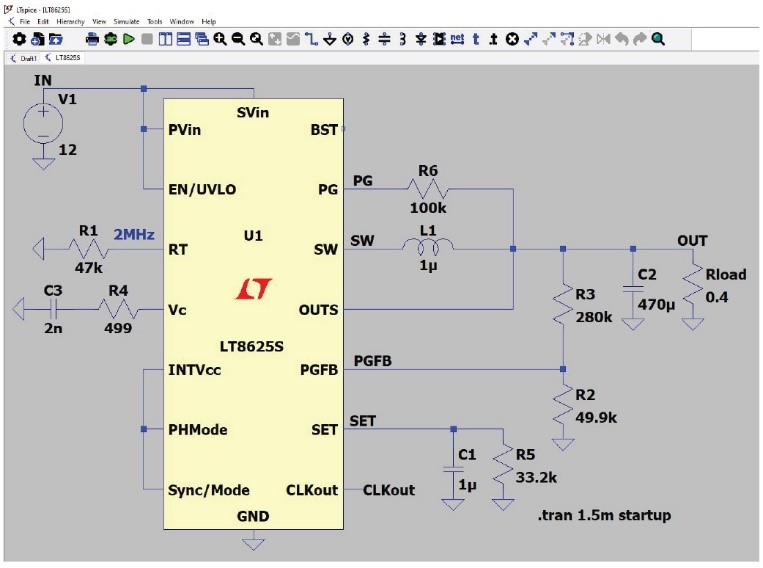
Figure 3 shows the LT8625S, a third-generation Silent Switcher switching regulator, modeled using the free simulation program LTspice®. This switch-mode power converter supports an input voltage of up to 18 V and can be operated with a load current of up to 8 A. It produces a low frequency noise of 4 μV rms between 10 Hz and 100 kHz on the output voltage. Additionally, it features a built-in precision current source with an accuracy of ±0.8% over the entire allowable temperature range of –40°C to +125°C.
Figure 3: A third-generation Silent Switcher switching regulator with unity-gain architecture.
In the circuit in Figure 3, the output voltage is set using resistor R5 on the SET pin. It’s important to note the presence of a resistor divider, composed of R3 and R2, between the output voltage and the PGFB pin. This resistor divider does not influence the control loop but is only used to operate the PG pin.
The design shifts from traditional and established methods like using a resistor divider in a control loop to more modern techniques such as unity-gain architecture. This advancement allows for the generation of significantly lower noise levels in the low frequency range. Moreover, the minimal noise that remains is not dependent on the set output voltage, enabling the creation of very low voltages down to 0 V. Many new linear regulators as well as switching regulators use this innovation.
About the Author
Frederik Dostal is a power management expert with more than 20 years of experience in this industry. After his studies of microelectronics at the University of Erlangen, Germany, he joined National Semiconductor in 2001, where he worked as a field applications engineer, gaining experience in implementing power management solutions in customer projects. During his time at National, he also spent four years in Phoenix, Arizona (U.S.A.), working on switch-mode power supplies as an applications engineer. In 2009, he joined Analog Devices, where he has since held a variety of positions working for the product line and European technical support, and currently brings his broad design and application knowledge as a power management expert. Frederik works in the ADI office in Munich, Germany.
Disclaimer: This article has been published with explicit permission from Analog Devices Inc. (ADI), who has granted Excelpoint the rights to produce and share this content on our platform. All information, insights, and viewpoints are provided in collaboration with ADI, ensuring authenticity and accuracy. No part of this article may be reproduced or utilized in any form or by any means without prior written consent from ADI and Excelpoint.