Analog Devices: Hardware Design Solution for Tumour Electric Field Therapy
Background Overview
Malignant tumours have long posed a significant public health challenge. Tumour Treating Fields (TTFields) therapy is an innovative and increasingly popular technology in the medical field. It employs wearable devices to emit low-intensity alternating electric fields at the tumour site, disrupting cancer cells and preventing them from dividing and proliferating normally, thus achieving an anti-cancer effect. This therapy is well-tolerated, with most side effects limited to mild skin irritation.
According to data released at the 2023 ASCO Annual Meeting, results from the LUNAR trial (NCT02973789) showed that for patients with metastatic non-small cell lung cancer (NSCLC), combining TTFields with standard lung cancer treatments (such as immunotherapy or chemotherapy) improves overall survival rates and reduces the risk of death compared to using standard treatment alone.
Programme Introduction
Excelpoint invited Engineer Huang from a long-term client company specializing in medical devices to share practical cases, leveraging his extensive industry experience.
Design Components
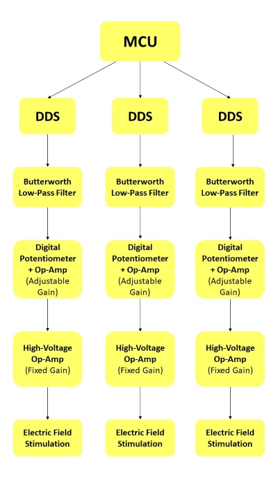
The TTFields therapy device discussed in this article primarily comprises a physiological signal detection system, an electric field stimulation system, and a data processing and analysis system. Known for its high precision and accuracy, this device was designed by Engineer Huang and his team using multiple ADI products. The hardware design solution for the electric field stimulation system is illustrated in Figure 1.
Figure 1. Hardware Design Solution for the Electric Field Stimulation System
Key Components and Their Implementation
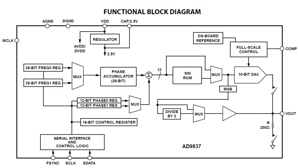
AD9837 DDS: In the electric field stimulation system, ADI’s AD9837, a low-power, programmable waveform generator, is used. It produces sine, triangular, and square wave outputs, with output frequency and phase easily programmed via software. Engineer Huang highlighted that the primary reason for using this chip is its high resolution, achieving 0.02Hz at a clock rate of 5MHz.
Figure 2: AD9837 Functional Block Diagram
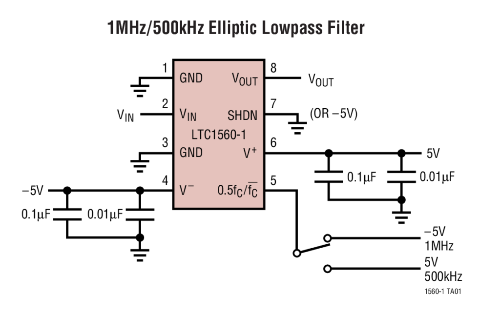
LTC1560-1 Elliptic Filter: The elliptic filter, ADI’s LTC1560-1, is a 5th-order, continuous-time, low-pass filter with selectable cutoff frequencies of 500kHz or 1MHz via pin selection. Designed for low noise and low distortion, it provides a signal-to-noise ratio (SNR) of 69dB and a total harmonic distortion (THD) of -63dB for a 1Vrms input signal.
Figure 3: Reference Circuit Design for LTC1560-1
AD5282 Digital Potentiometer and ADA4805-2 Op-Amp: The AD5282 is a dual-channel, 256-position, I2C-compatible digital potentiometer paired with the ADA4805-2, a high-speed, low-power (500µA) voltage feedback op-amp with rail-to-rail output. The op-amp offers a 105MHz bandwidth (gain of 1), 160V/µs slew rate, and 125µV low input offset voltage. Together, they provide adjustable output voltage gain while maintaining input signal integrity.
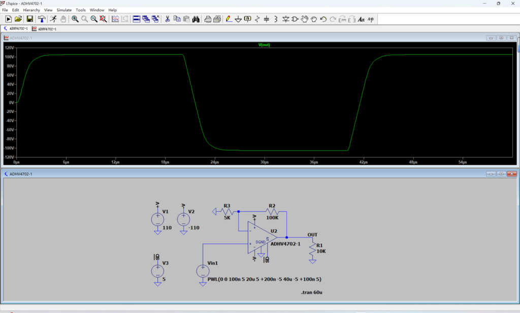
ADHV4702-1 High-Voltage Op-Amp: For high-voltage signal amplification, the ADHV4702-1 features a ±110V supply voltage and a high slew rate of 74V/µs. Its high precision includes a 170dB open-loop gain (AOL), 160dB common-mode rejection ratio (CMRR), 2µV/°C input offset voltage (VOS) drift, and 8 nV/√Hz input voltage noise. The simulation for generating adjustable ±110V pulses using the ADHV4702-1 is shown in Figure 4.
Figure 4:Simulation of ±110V Pulse Signal Using ADHV4702-1
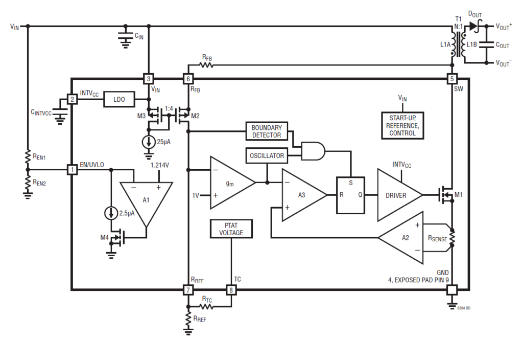
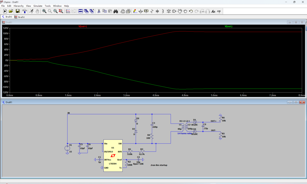
LT8304 Power Supply: The LT8304, a monolithic, low-power, isolated flyback converter, regulates output voltage by sampling the primary-side flyback waveform, eliminating the need for a third winding or optocoupler. It operates in boundary mode for excellent load regulation and burst mode for high efficiency at light loads, minimizing output ripple. The LT8304-1 supports a 3V to 100V input range and delivers up to 24W of isolated output power, as illustrated in Figure 6.
Figure 5: LT8304 Block Diagram
Figure 6: Simulation of ±110V High Voltage Output Using LT8304
Practical Considerations
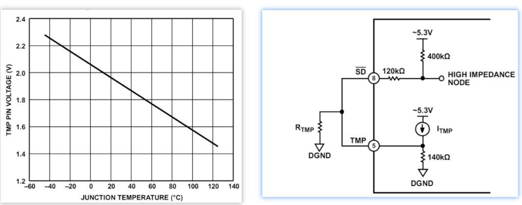
When applying the ADHV4702-1, consider utilizing the TMP pin for temperature monitoring and proper heat dissipation. The TMP pin tracks temperature changes with a typical voltage of 1.9 V at room temperature, varying by approximately -4.5 mV/°C. To prevent overheating, connect the TMP pin directly to the SD pin and ground it through a resistor (RTEMP). Adjusting the value of RTEMP sets the thermal shutdown threshold, as shown in Figure 7.
In PCB design, add an exposed copper top layer beneath the chip for heat management. Solder the chip’s exposed pad (EPAD) to this layer for optimal heat dissipation. Connect the top exposed copper area to the bottom exposed copper ground plane through an array of thermal vias. Additionally, attaching a heatsink to the bottom exposed ground plane can further enhance heat dissipation.
Summary
This article covers the hardware design for tumour electric field therapy using ADI components known for their low power consumption, high precision, and compact size. A key feature is the LT8304, which boosts high-voltage power and samples isolated output voltage directly from the primary flyback waveform, eliminating the need for a third winding or optocoupler.
The ADHV4702-1 high-voltage op-amp is ideal for tumour treatment equipment due to its high input impedance, low input bias current, low offset voltage, low drift, and low noise. It operates with ±110V symmetrical dual power supplies, asymmetrical dual power supplies, or a single 220V power supply, benefiting from ADI’s advanced semiconductor process and innovative architecture.
Disclaimer: This article is published by Excelpoint. All information, insights, and viewpoints are provided in collaboration with ADI, ensuring authenticity and accuracy. No part of this article may be reproduced or utilized in any form or by any means without prior written consent from ADI and Excelpoint.